Understanding MMIO-Based Device Register Access
How a Linux device driver maps register offsets through MMIO, the MMU, and the system interconnect for on-chip and PCIe devices.
Hardware devices such as AI accelerators expose registers for control, status reporting, command submission, and interrupt handling. A driver accesses these registers through Memory-Mapped I/O (MMIO), but a register offset such as 0x0100 is not an address by itself. It becomes accessible only after software combines it with a mapped MMIO base address.
This post follows one register access from a Linux driver to the hardware and compares how the same model applies to on-chip and PCIe devices.
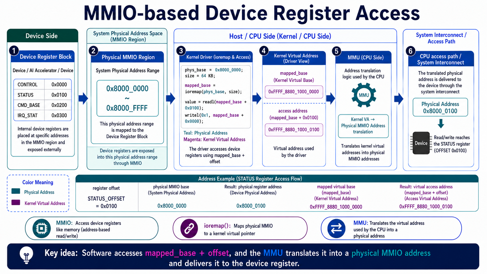
1. Register Blocks and Offsets
A device implements an internal register block. For example:
CONTROL   offset 0x0000
STATUS    offset 0x0100
CMD_BASE  offset 0x0200
IRQ_STAT  offset 0x0300
Each value is a register offset, not a complete physical or virtual address. The device contains address-decoding logic that selects a register based on this offset. An access at offset 0x0100, for example, selects the STATUS register.
The address of a register is therefore calculated relative to the beginning of its MMIO region:
Register address = MMIO base address + register offset
This distinction matters because hardware documentation commonly lists register offsets while the operating system manages the base address separately.
2. The Physical MMIO Region
The system exposes the device’s register block through a range in its physical address space. Suppose an accelerator is assigned the following region:
Physical MMIO base: 0x8000_0000
MMIO region size:   64 KB
Address range:      0x8000_0000–0x8000_FFFF
The physical address of the STATUS register is:
Physical MMIO base         0x8000_0000
STATUS register offset     0x0000_0100
                           --------------
Physical register address  0x8000_0100
An access to physical address 0x8000_0100 is routed to the device rather than DRAM. After the transaction reaches the device, its register decoder interprets the address as MMIO base + 0x0100 and selects STATUS.
3. Why the Driver Maps MMIO
When the MMU is enabled, CPU instructions normally operate on virtual addresses. A Linux kernel driver therefore should not treat a raw physical MMIO address as an ordinary C pointer. It first maps the physical region into the kernel virtual address space.
Conceptually, the driver could perform the following mapping:
phys_base = 0x80000000;
size = 64 * 1024;

mapped_base = ioremap(phys_base, size);
Assume that ioremap() returns 0xFFFF_8880_1000_0000. The driver can then access STATUS at offset 0x0100:
status = readl(mapped_base + 0x0100);
The resulting relationship is:
Kernel VA  0xFFFF_8880_1000_0100
                       ↓ MMU translation
Physical   0x0000_0000_8000_0100
ioremap() does not copy device registers into RAM. It creates a virtual mapping that refers to the physical MMIO range, preserving the same offset on both sides.
4. From a Driver Access to a Device Register
Consider the following operation:
status = readl(mapped_base + STATUS_OFFSET);
The complete path is:
Linux device driver
        ↓ readl(mapped_base + STATUS_OFFSET)
Kernel virtual address
        ↓ MMU and kernel page tables
Physical MMIO address
        ↓ system interconnect routing
Device MMIO interface
        ↓ register offset decoding
STATUS register
Each component has a distinct responsibility.
4.1 MMU Translation
The MMU translates the kernel virtual address into a physical address by consulting the kernel page tables. It does not know that the result represents a device or the STATUS register; it only performs address translation and applies the mapping’s memory attributes.
4.2 System Interconnect Routing
The system interconnect decodes the resulting physical address and routes the transaction to its destination. An on-chip device may be reached through an AXI fabric or Network-on-Chip (NoC), while a PCIe device is reached through a Root Complex and PCIe link.
4.3 Device Register Decoding
Once the transaction arrives, the device determines the offset within its MMIO window and selects the corresponding register. The device, rather than the MMU, understands that offset 0x0100 refers to STATUS.
5. Using readl() and writel()
Linux drivers generally use MMIO accessors instead of dereferencing the mapped address as a normal pointer:
value = readl(mapped_base + STATUS_OFFSET);
writel(0x1, mapped_base + CONTROL_OFFSET);
These accessors provide architecture-appropriate I/O semantics and help preserve the required ordering and device-memory behavior. That is important because register accesses can have hardware side effects:
- Writing
CONTROL = 1may start the accelerator. - Reading
IRQ_STATmay return pending interrupt status. - Writing
IRQ_STATmay acknowledge or clear an interrupt. - Writing a doorbell register may notify the device of a new command.
Register definitions and the device specification determine the exact behavior, so MMIO must not be treated like ordinary RAM.
6. On-Chip Accelerator Access
An on-chip accelerator is an IP block inside the same SoC as the CPU. Its register region is normally part of the SoC physical memory map:
0x0000_0000–0x3FFF_FFFF  DRAM
0x4000_0000–0x4000_FFFF  UART
0x5000_0000–0x5000_FFFF  AI accelerator MMIO
The driver may obtain this resource from Device Tree, ACPI, or platform data. A common platform-driver flow is:
Device Tree / ACPI
        ↓
Platform device resource
        ↓ devm_ioremap_resource()
Kernel virtual MMIO base
After the mapping is established, a register access travels approximately as follows:
CPU → MMU → AXI / NoC → accelerator register block
This path does not require PCIe enumeration or a PCIe Base Address Register (BAR).
7. PCIe Accelerator Access
A PCIe accelerator exposes one or more BARs in its PCIe configuration space. A BAR describes the size and type of an address window required for registers or device memory. During PCIe enumeration, the host assigns a physical address range to that window.
For example, if the device requests a 64 KB BAR0, the host might assign:
BAR0 physical range: 0x8000_0000–0x8000_FFFF
The driver can map BAR0 with a PCI-specific mapping API:
mapped_base = pci_iomap(pdev, 0, 0);
A subsequent access travels through the PCIe hierarchy:
CPU
 ↓ MMU
Host system interconnect
 ↓
PCIe Root Complex
 ↓ PCIe Memory Read / Write
Endpoint BAR match
 ↓
Accelerator register block
When the endpoint receives a transaction for BAR0 + 0x0100, it decodes the offset and selects STATUS, just as an on-chip device does within its own MMIO window.
8. On-Chip MMIO vs. PCIe MMIO
| Aspect | On-Chip Accelerator | PCIe Accelerator |
|---|---|---|
| Physical connection | Same SoC | PCIe endpoint |
| MMIO resource origin | SoC physical memory map | Host-assigned PCIe BAR |
| Resource description | Device Tree, ACPI, or platform data | PCIe configuration space |
| Common mapping API | devm_ioremap_resource() or ioremap() | pci_iomap() or a managed PCI mapping API |
| Hardware path | CPU → AXI/NoC → device | CPU → Root Complex → PCIe → endpoint |
| PCIe enumeration | Not required | Required |
| Driver access form | mapped_base + offset | mapped_base + offset |
MMIO is not synonymous with PCIe. A PCIe BAR is one mechanism for exposing an MMIO range, while an on-chip device can expose one directly through the SoC memory map. The transport and resource-discovery methods differ, but the driver’s mapped-base-plus-offset programming model remains similar.
9. Summary
MMIO-based register access connects a device’s internal register block to software through several layers:
- The device implements registers at defined offsets.
- The system exposes the register block through a physical MMIO region.
- The driver obtains the region’s physical base address and size.
- The driver maps that region into kernel virtual address space.
- The driver uses
readl()orwritel()withmapped_base + offset. - The MMU translates the kernel virtual address into a physical MMIO address.
- The interconnect routes the transaction to the device.
- The device decodes the offset and performs the register access.
The central idea is:
Software accesses
mapped_base + offset; the MMU translates that virtual address into a physical MMIO address, and the system routes the transaction to the corresponding device register.
On-chip and PCIe accelerators establish and transport MMIO transactions differently, but both ultimately use this same register-access model.